Applied Materials Introduces New Technologies and Capabilities for Accelerating the Semiconductor Industry’s Heterogeneous Integration Roadmap
- New advanced software modeling and simulation for die-to-wafer hybrid bonding at Applied’s
Advanced Packaging Development Center speeds customer time to market - Enters into joint development agreement with
EV Group for co-optimized wafer-to-wafer hybrid bonding solutions - Enables larger, higher quality substrates for advanced packaging through the recent acquisition of Tango Systems, a leader in panel-level processing
- Provides customer access to large-area yield management solutions and other technologies from its Display business
Applied is combining its leadership technologies in advanced packaging and large-area substrates with industry collaborations to speed the availability of solutions that deliver simultaneous improvements in power, performance, area, cost and time to market (PPACt™).
Heterogeneous integration brings new kinds of design and manufacturing flexibility to semiconductor and system companies by allowing chips of various technologies, functions and sizes to be integrated in one package. Applied is already the largest supplier of advanced packaging technologies with optimized products spanning etch, physical vapor deposition (PVD), chemical vapor deposition (CVD), electroplating, surface treatments and annealing. Applied’s
“Applied’s industry-leading portfolio of advanced packaging solutions gives customers the broadest selection of enabling technologies for heterogenous integration,” said
Today, Applied is unveiling innovations in three areas critical to advanced packaging for heterogeneous integration: die-to-wafer hybrid bonding, wafer-to-wafer bonding and advanced substrates.
Accelerating Die-to-Wafer Hybrid Bonding
Die-to-wafer hybrid bonding uses direct, copper-to-copper interconnects to increase I/O density and shorten the wiring length between chiplets to improve overall performance, power and cost. To accelerate development of this technology, Applied is adding advanced software modeling and simulation to its
“Our joint development program with
Developing Co-optimized Solutions for Wafer-to-Wafer Hybrid Bonding
Wafer-to-wafer bonding enables chipmakers to build certain chip structures on one wafer and others on a second wafer and then bond the wafers to create complete devices. In order to achieve high performance and yield, the quality of the front-end processing steps is critical as is the precise uniformity and alignment of the wafers as they are being bonded. Applied today announced a joint development agreement with
“Semiconductor innovation is increasingly being fueled by 3D integration and engineered materials, which drives greater demand for wafer-to-wafer hybrid bonding. Optimizing this critical process for new applications requires an in-depth understanding of integration issues both up and down the process chain,” said Dr.
“Through collaborations with industry partners including Besi and EVG,
Larger, More Advanced Substrates Deliver PPAC Benefits
The need for more advanced substrates is increasing as chipmakers squeeze greater numbers of chips into sophisticated 2.5D and 3D package designs. To enable larger package sizes with greater interconnect density, Applied is using state-of-the-art panel-level processing technology from its recent acquisition of Tango Systems. Panel-size substrates, which can measure 500mm x 500mm or larger, can accommodate a greater number of packages compared to wafer-size formats, thereby providing a cost benefit in addition to better power, performance and area.
As its customers adopt these larger panel sizes, Applied is providing them with access to large-area materials engineering technologies from its
Additional details on Applied’s packaging technologies will be discussed at the company’s 2021 ICAPS and Packaging
About Applied Materials
A photo accompanying this announcement is available at https://www.globenewswire.com/NewsRoom/AttachmentNg/15b9874b-cdab-4956-bbc5-ad9c59fc0f4c
Contact:

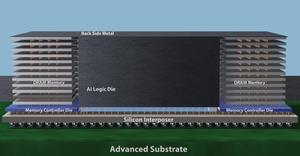
Accelerating Heterogeneous Design and Integration
Heterogeneous integration brings new kinds of design and manufacturing flexibility to semiconductor and systems companies by allowing chips of various technologies, functions and sizes to be integrated in one package. Applied Materials is combining its leadership in process technology and large-area substrates along with ecosystem collaborations to accelerate the industry’s heterogeneous design and integration roadmaps.
Source: Applied Materials, Inc.

