Applied Materials Solves Major Bottleneck to Continued 2D Scaling
|
|||||
Applied’s new Selective Tungsten process technology gives chipmakers a new way to build transistor contacts, which are the crucial, first level of wiring that connects the transistor to the rest of the wiring in the chip. The selective deposition innovation lowers contact resistance which impedes transistor performance and increases power consumption. With this technology, node scaling of transistors and their contacts can continue to 5nm, 3nm and below, enabling simultaneous advances in chip power, performance and area/cost (PPAC).
Scaling Challenge
While advances in lithography have helped shrink the transistor contact vias, the traditional approach to filling the vias with contact metal has become a critical bottleneck to PPAC.
Traditionally, the transistor contacts have been formed in a multi-layer process. The contact via is first lined with an adhesion and barrier layer made of titanium nitride, then a nucleation layer is deposited, and finally the remaining space is filled with tungsten, which is the contact metal of choice due to its low resistivity.
At the 7nm foundry node, the contact via is only about 20nm in diameter. The liner-barrier and nucleation layers occupy approximately 75 percent of the via’s volume, leaving only around 25 percent of the volume for tungsten. The thin tungsten wire has very high contact resistance, and this creates a major bottleneck to PPAC and further 2D scaling.
“With the arrival of EUV, we need to solve some critical materials engineering challenges to enable 2D scaling to continue,” said
Selective Tungsten Deposition
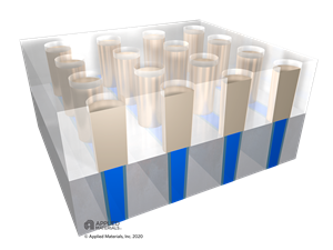
Applied’s new Endura® Volta™ Selective Tungsten CVD system enables chipmakers to selectively deposit tungsten in the transistor contact vias, eliminating the liner-barrier and nucleation layers. The entire via is filled with low-resistance tungsten, and the bottleneck to continued PPAC scaling is removed.
Applied’s Selective Tungsten technology is an Integrated Materials Solution that combines multiple process technologies in a pristine, high-vacuum environment that is many times cleaner than the cleanroom itself. Atomic-level surface treatments are applied to the wafer, and a unique deposition process is employed so that tungsten atoms are selectively deposited in the contact vias, creating a perfect bottom-up fill with no delamination, seams or voids.
“For decades, the industry could count on 2D scaling to drive simultaneous improvements in power, performance and area/cost,” said
The new Endura system has been selected by multiple leading customers worldwide. It is the latest addition to Applied’s portfolio of innovative selective process technologies which include selective epitaxy, selective deposition and selective removal. These selective processes allow chipmakers to create, shape and modify materials in entirely new ways to enable continued advances in PPAC.
About Applied Materials
Contact:
A photo accompanying this announcement is available at https://www.globenewswire.com/NewsRoom/AttachmentNg/e80b0739-8446-40c0-9bd2-cff27cd407f0
The photo is also available at Newscom, www.newscom.com, and via AP PhotoExpress.
Source: Applied Materials, Inc.

